Intel’s 14A Node: Latest Yield Insights and Manufacturing Progress
Recent research from Morgan Stanley, a prominent investment bank, has provided new insights into Intel’s 14A semiconductor manufacturing node. According to the report, Intel’s 14A node currently exhibits a defect density (D0) of 0.5. In semiconductor fabrication, this figure represents the number of defects per square centimeter, and a D0 of 0.5 indicates a relatively low occurrence of non-functional silicon during production. This suggests that the 14A node is still in the early stages of its manufacturing ramp, but the initial results are promising.
Notably, the report confirms that the 14A node is already outperforming the 18A node at a comparable point in its development timeline. Intel has set ambitious targets for the 14A node, aiming to reduce the defect rate to between 0.1 and 0.2 by the first quarter of 2027. At that stage, Intel plans to begin running internal test chips and initiate a limited ramp for its own products. Risk production is scheduled for 2028, with high-volume manufacturing expected to follow in 2029.
Yield Estimates and Die Size Analysis
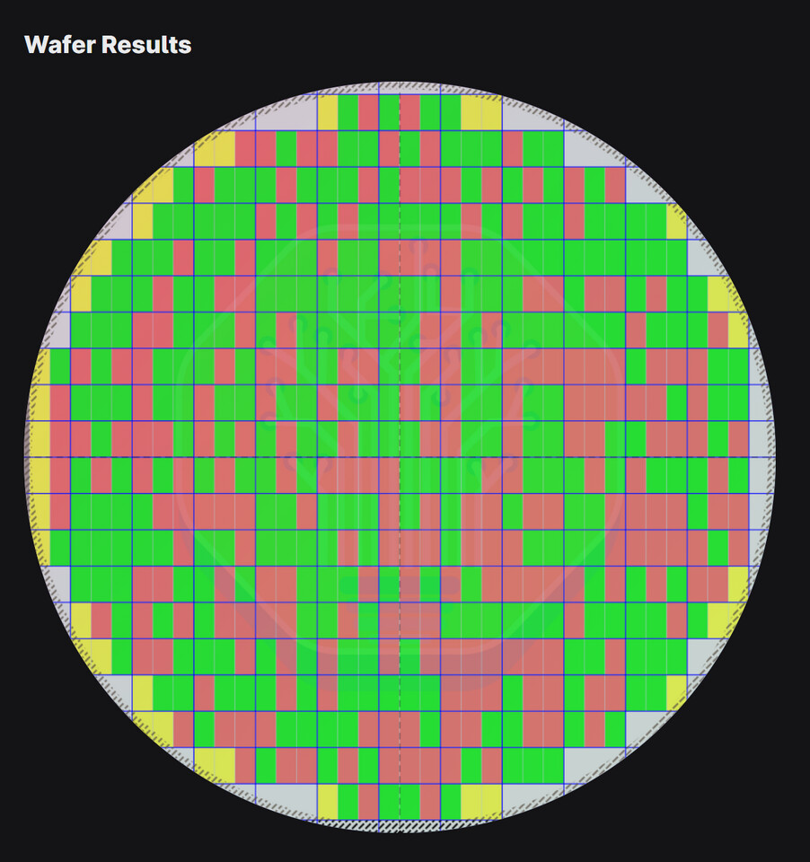
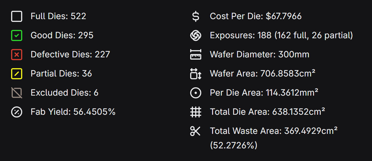
Examining Intel’s current “Panther Lake” system-on-chip (SoC) provides further context for these developments. The Panther Lake SoC integrates multiple smaller dies into a single package, with the compute tile produced using the 18A node. This compute tile measures approximately 8.004 x 14.288 mm, resulting in a silicon area of 114.304 mm².
If a die of this size were manufactured on the 14A node using current process parameters, the estimated yield would be around 56.45%. This calculation assumes the use of High-NA EUV half-field exposures and is based on the Poisson yield model, which is commonly used in the semiconductor industry. While the 18A node currently delivers higher yields due to its mature, high-volume production, the early yield statistics for 14A are encouraging.
Morgan Stanley’s report also notes that yield for a larger test chip on the 14A node is about 40%, suggesting that die size significantly impacts yield outcomes. As Intel continues to refine the 14A process and reduces the defect rate to the targeted 0.1–0.2 range, yields for dies around 100 mm² could reach 80–90%, depending on the specific design. It is important to note that these figures only account for the Poisson yield model; actual production yields also depend on parametric yield, which measures the proportion of chips that meet all functional requirements. Detailed parametric yield data is typically proprietary and not publicly disclosed.
Process Development and Equipment Advances
Intel’s 14A node is currently at the 0.5 Process Design Kit (PDK) stage. The PDK is a critical set of files and documentation that enables customers to design chips for a specific manufacturing process. Final decisions on volume production and design requirements are expected when the 0.9 PDK is released, which industry veteran Lip-Bu Tan has described as a “holy grail” milestone. The 0.9 PDK for the 14A node is anticipated to be available in October.
In partnership with ASML, Intel has completed acceptance testing for the 14A node at its foundry, leveraging advanced High-NA EUV lithography equipment. The TWINSCAN EXE:5200B, ASML’s second-generation High-NA EUV scanner, follows the earlier TWINSCAN EXE:5000 used in initial 14A trial runs. Intel has reported processing over 30,000 wafers in a single quarter, with significant improvements in manufacturing efficiency. The company has managed to reduce the number of process steps required for certain layers from 40 to fewer than 10, resulting in much faster cycle times and streamlined production.
These advancements highlight Intel’s ongoing commitment to pushing the boundaries of semiconductor manufacturing. As the 14A node continues to mature, further improvements in yield and process efficiency are expected, positioning Intel to remain competitive in the rapidly evolving chip industry.