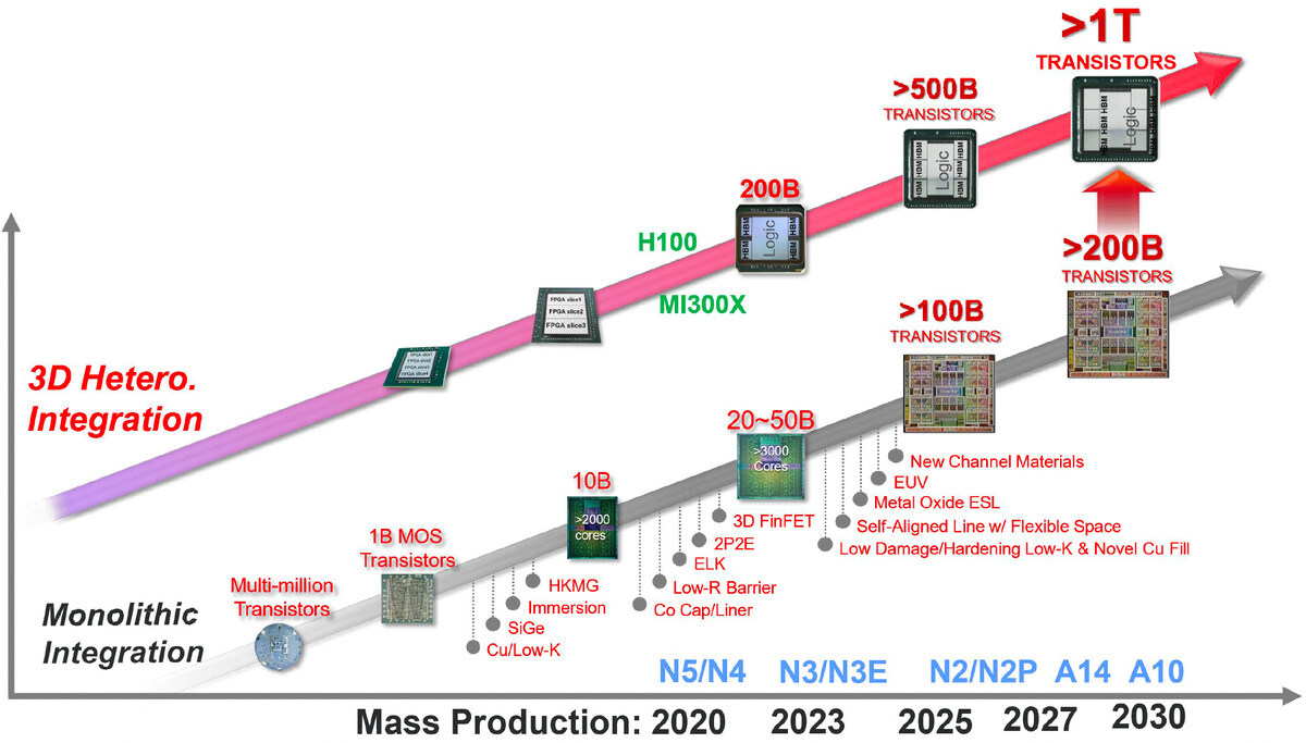
During the recent IEDM conference, TSMC provided a preview of its process roadmap for delivering next-generation chip packages with over one trillion transistors by 2030. This aligns with Intel's similar long-term visions. The increased transistor counts will be achieved through advanced 3D packaging of multiple chipsets. However, TSMC also aims to increase the complexity of monolithic chips, enabling designs with 200 billion transistors on a single die. This will require steady enhancement of TSMC's planned N2, N2P, N1.4, and N1 nodes, which are expected to be released between now and the end of the decade. While multi-chipset architectures are currently gaining popularity, TSMC emphasizes the need for both packaging density and raw transistor density to scale up together. To put TSMC's goals into perspective, NVIDIA's GH100 GPU, which has 80 billion transistors, is one of the largest chips today, excluding wafer-scale designs from Cerebras.
However, TSMC's roadmap goes beyond doubling that number, with plans for monolithic designs with over 100 billion transistors and eventually reaching 200 billion transistors. As die sizes increase, yields become more challenging, which is where advanced packaging of smaller chiplets becomes crucial. AMD's MI300X and Intel's Ponte Vecchio already integrate dozens of tiles in their multi-chip module offerings, with Ponte Vecchio having 47 tiles. TSMC envisions chip packages that house more than a trillion transistors through technologies like CoWoS, InFO, 3D stacking, and others. While the scaling cadence has recently slowed, TSMC remains confident in achieving breakthroughs in both packaging and process to meet future density demands. The continuous investment by the foundry ensures progress in unlocking next-generation semiconductor capabilities. However, the timeline is ultimately dictated by physics, regardless of how ambitious the roadmap may be.