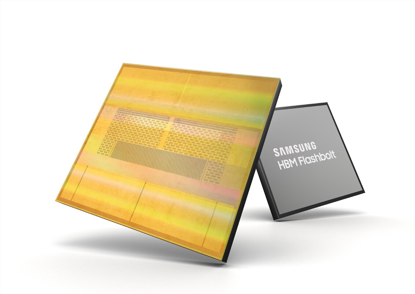
According to a blog post on the Samsung blog by SangJoon Hwang, Executive Vice President and Head of the DRAM Product & Technology Team at Samsung Electronics, High-Bandwidth Memory 4 (HBM4) is set to be released in 2025. The development of HBM memory has progressed over the years, starting with its introduction in 2015 with the AMD Radeon R9 Fury X. The second-generation HBM2 was seen in the NVIDIA Tesla P100 in 2016, and the third-generation HBM3 was introduced with the NVIDIA Hopper GH100 GPU in 2022. Samsung has currently developed 9.8 Gbps HBM3E memory, which will soon be available for sampling to customers.
However, Samsung has set more ambitious goals for this development cycle and plans to announce HBM4 in 2025, with the possibility of commercial products being available in the same year. Notably, HBM4 memory will feature technology optimized for high thermal properties, including non-conductive film (NCF) assembly and hybrid copper bonding (HCB). The NCF is a polymer layer that enhances the stability of micro bumps and TSVs in the chip, providing protection against shock for memory solder bump dies. Hybrid copper bonding is an advanced semiconductor packaging method that enables direct copper-to-copper connections between semiconductor components, allowing for high-density, 3D-like packaging. It offers increased I/O density, improved bandwidth, and enhanced power efficiency. Instead of regular micro bumps, it utilizes a copper layer as a conductor and oxide insulator to achieve the necessary connection density for HBM-like structures.
