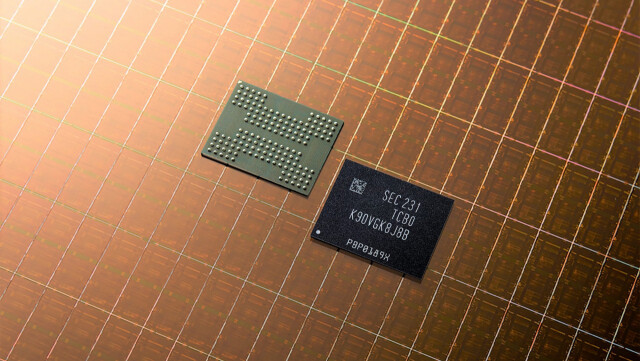
According to reports from South Korea, Samsung is poised to surpass SK Hynix in the race to develop NAND Flash with over 300 layers. The Seoul Economic Daily claims that Samsung will have a 300+ layer V-NAND chip ready for production in 2024, potentially beating SK Hynix by a year. Currently, Samsung's most advanced stacked NAND has 236 layers, which is four more than Micron and YMTC, but two less than SK Hynix.
What stands out in the Seoul Economic Daily report is that Samsung will stick with two stacks, unlike SK Hynix's triple stack approach. This means that Samsung aims for over 150 layers of NAND per stack, which poses a risk in terms of yields. The taller the stacks, the higher the chance of a failed stack. However, Samsung may have found a solution to mitigate this issue. While modern 3D NAND technology allows for denser stacks compared to the past, this is still a significant risk for Samsung. Nevertheless, given the current low demand and news of production cutbacks, it may be an opportune time for Samsung to utilize its fabs to test this densely stacked NAND and assess its mass production feasibility.
Samsung's roadmap envisions a V-NAND product with over 1000 layers by 2030. However, it is evident that the journey towards achieving this goal is still long and complex.