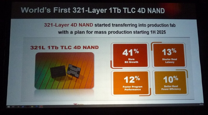
Courtesy of a keynote speech by SK Hynix at the Flash Memory Summit, we now have more details about their upcoming 321-layer NAND Flash. PC Watch Japan, who attended the industry event, shared some pictures from the keynote that provide crucial details missing from last week's press release. According to SK Hynix's official performance figures, we can expect up to a 12% increase in program performance, specifically in write performance, and up to a 13% improvement in read latency. However, these performance metrics will depend on the SSD controller the NAND is paired with and the related firmware on that controller.
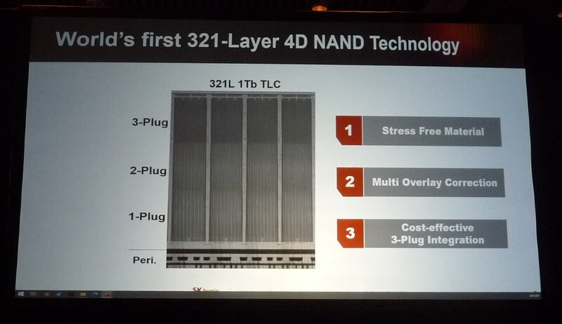
PC Watch Japan also reports a program throughput of 194 MB/s, which is a 26 MB/s improvement over SK Hynix's 176-layer NAND and currently the highest known program throughput of any announced NAND Flash. However, Kioxia is expecting to achieve 205 MB/s with its next generation of 300-layer NAND. SK Hynix also claims a 10% improvement in read power efficiency, although this is not significant for modern SSDs unless we are referring to server-level SSDs with multiple NAND chips. Instead of using two stacks of 150+ layers each, SK Hynix opted for three stacks of 107 layers, which should be compared to their current 238-layer product with two stacks of 119 layers. This decision made it easier to produce the new NAND package and is expected to result in higher yields in the long term. Each NAND package is projected to have a memory density of 20 Gbit per square millimeter or more, nearly double that of their 176-layer NAND.