TSMC’s 2nm Node Sees Unprecedented Demand from Major Clients
TSMC’s advanced 2nm semiconductor process node is attracting remarkable interest from industry leaders, signaling a significant shift in chip design priorities. According to Kevin Zhang, TSMC’s Senior Vice President, the company’s N2 node has already achieved four times the number of tape-outs compared to its previous flagship 3nm N3 node. This surge highlights a strong commitment from TSMC’s long-standing partners, who are now prioritizing 2nm chip development over 3nm process design kits (PDKs).
Breakthroughs in Power Efficiency and Performance with GAAFET
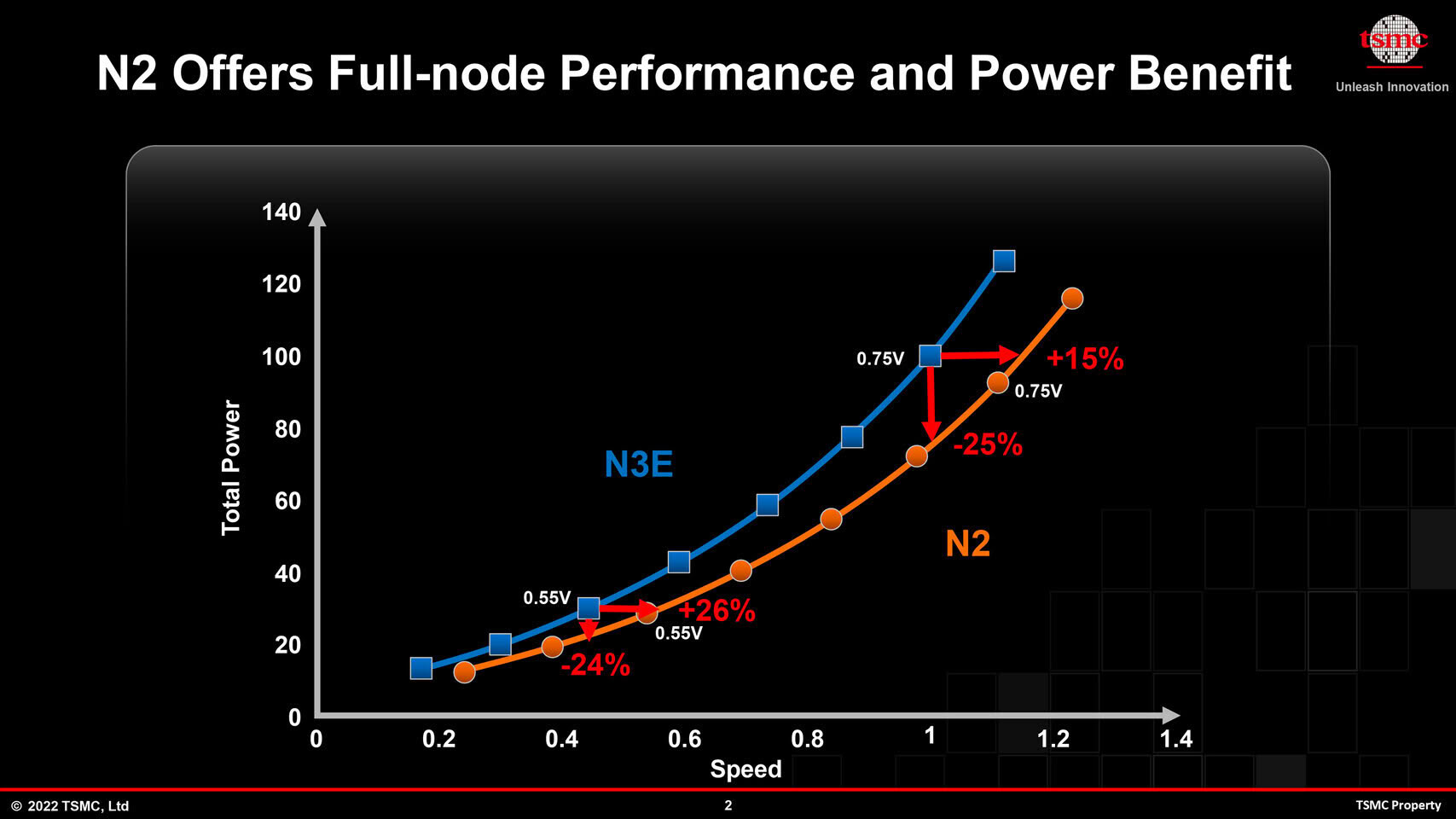
The primary driver behind this rapid adoption is the introduction of TSMC’s first gate-all-around FET (GAAFET) nanosheet transistor technology. The N2 node delivers up to a 15% performance boost at the same power level, or up to a 30% reduction in power consumption at the same speed, compared to the previous N3E node. This advancement enables chip designers to achieve higher switching speeds within existing power budgets or significantly lower energy usage while maintaining performance targets.
Additionally, the N2 node offers a 15% increase in transistor density. This improvement allows for either smaller chip dies with equivalent functionality or larger dies that deliver enhanced performance, providing greater flexibility for semiconductor designers.
Market Impact and Revenue Trends
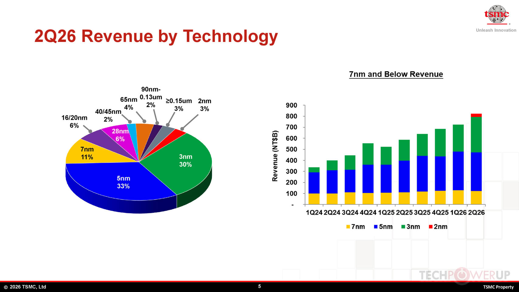
TSMC began high-volume manufacturing of its N2 node in the fourth quarter of 2025. Despite this, the 2nm node currently accounts for just 3% of the company’s revenue, while the 3nm and 5nm nodes represent 30% and 33% respectively. However, this distribution is expected to shift as more customers ramp up production and shipments of 2nm chips increase.
Notable clients adopting the N2 node include AMD, with its EPYC “Venice” server CPUs, and Apple, which is utilizing the technology for its A20 Pro chips in the upcoming iPhone 18 Pro series. With four times as many tape-outs on the 2nm node compared to 3nm, TSMC is poised for record-breaking quarterly results as the node’s adoption accelerates.
Each new process generation brings increased wafer costs due to greater manufacturing complexity. As a result, the surge in 2nm tape-outs is expected to significantly boost TSMC’s revenue in the coming quarters.
Future Roadmap for TSMC’s 2nm Family
Looking ahead, TSMC plans to expand its 2nm process portfolio with several new variants. The N2P node is set to follow the initial N2 rollout in the second half of this year, promising further enhancements in performance and power efficiency. In 2027, TSMC will introduce the N2X node, with the N2U variant scheduled for 2028. While specific use cases for these upcoming nodes will become clearer closer to their launch dates, TSMC aims to ensure that the 2nm family remains a cornerstone of its advanced manufacturing processes for years to come.