Researchers at MIT have developed a new technology that allows for the growth of 2D transition metal dichalcogenide (TMD) materials directly on fully fabricated silicon chips, enabling denser integrations. Traditional methods require temperatures of around 600°C, which can damage silicon transistors and circuits as they break down above 400°C. The MIT team overcame this challenge by creating a low-temperature growth process that preserves the chip's integrity, allowing 2D semiconductor transistors to be directly integrated on top of standard silicon circuits.
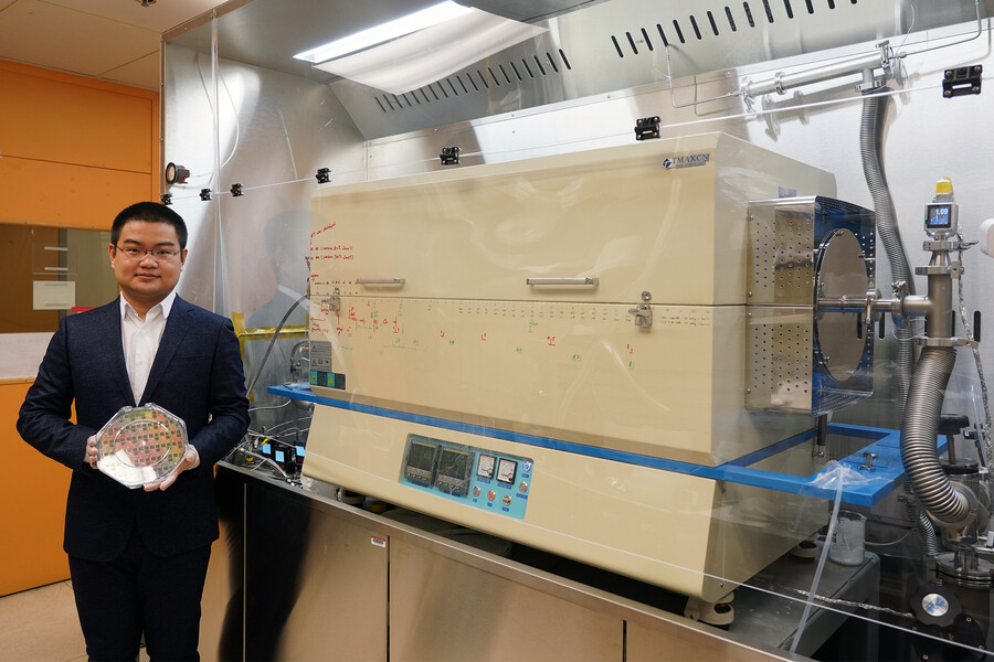
The new approach grows a smooth, highly uniform layer across an entire 8-inch wafer, unlike previous methods that involved growing 2D materials elsewhere before transferring them to a chip or wafer. This process often led to imperfections that negatively impacted device and chip performance. Additionally, the novel technology can grow a uniform layer of TMD material in less than an hour over 8-inch wafers, a significant improvement from previous methods that required over a day for a single layer. The enhanced speed and uniformity of this technology make it suitable for commercial applications, where 8-inch or larger wafers are essential.
The researchers focused on molybdenum disulfide, a flexible, transparent 2D material with powerful electronic and photonic properties ideal for semiconductor transistors. They designed a new furnace for the metal-organic chemical vapor deposition process, which has separate low and high-temperature regions. The silicon wafer is placed in the low-temperature region while vaporized molybdenum and sulfur precursors flow into the furnace. Molybdenum remains in the low-temperature region, while the sulfur precursor decomposes in the high-temperature region before flowing back into the low-temperature region to grow molybdenum disulfide on the wafer surface.
Emerging applications such as AI, automotive, and HPC require computing to be very dense, and stacking the transistors can be challenging. This new method has significant implications for the industry, enabling rapid, efficient integration of 2D materials into industrial fabrications. Future developments include fine-tuning the technique to grow multiple layers of 2D transistors and exploring low-temperature growth processes for flexible surfaces, such as polymers, textiles, or even paper.