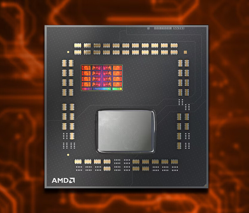
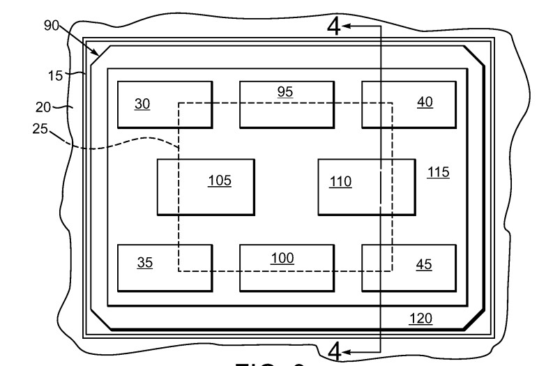
AMD has recently submitted a patent that outlines their plans to incorporate "multi-chip stacking" in upcoming Ryzen SoCs. According to a report by Wccftech, a post on X from @coreteks stated: "A new patent from AMD reveals the potential appearance of future Zen SoCs. Essentially, it is a unique packaging design that allows for compact chip stacking and interconnection by overlapping them partially, as shown in this diagram. The dashed line represents a larger die stacked on top of the smaller ones." The patent describes a fresh approach where smaller chiplets partially overlap with a larger die, creating space for additional components and functions on the same die. This method aims to enhance the efficiency of the contact area, making way for higher core counts, larger caches, and increased memory bandwidth within the same die size. The proposed stacking will decrease the physical distance between components by overlapping chiplets, reducing interconnect latency and enabling faster communication between different chip parts. Additionally, the design will enhance power management, as the separate chiplets allow for improved control of each unit through power gating.
Despite Intel losing some momentum (and market share) this year, AMD's opportunity to advance their goal of becoming the market leader lies in their commitment to innovation. Just as their 3D V-Cache technology propelled the success of the X3D processor lineup, this chip stacking approach could play a significant role in future AMD Ryzen SoCs. It appears that AMD is dedicated to moving away from the era of monolithic design and embracing the path of multi-chiplet technology; however, it may be a considerable time before (and if) this chip stacking transitions from patents to design, production, and final product.

