TSMC and NVIDIA Collaboration in Semiconductor Manufacturing
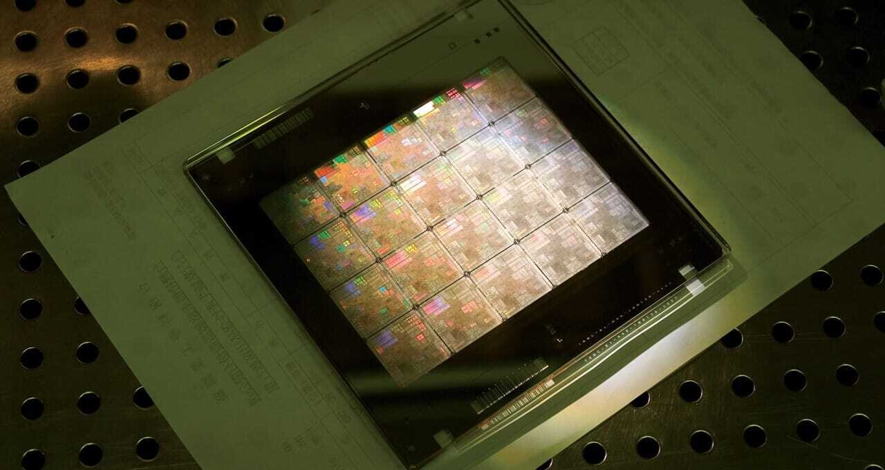
TSMC, a global leader in semiconductor manufacturing, is implementing NVIDIA's cuLitho computational lithography platform to enhance production efficiency and push the boundaries of physics in the development of advanced semiconductor chips. Computational lithography plays a crucial role in the chip manufacturing process by transferring circuitry onto silicon. This process involves intricate computations that encompass electromagnetic physics, photochemistry, computational geometry, iterative optimization, and distributed computing. Despite the significant computational resources dedicated to this step, it has traditionally been a bottleneck in introducing new technology nodes and computer architectures to the market.
Computational lithography represents the most compute-intensive workload in the semiconductor design and manufacturing process, consuming billions of hours annually on CPUs in cutting-edge foundries. A single mask set for a chip can require over 30 million hours of CPU compute time, necessitating large data centers within semiconductor foundries. With the introduction of accelerated computing, 350 NVIDIA H100 Tensor Core GPU-based systems can now replace 40,000 CPU systems, resulting in faster production times, cost savings, and reduced space and power consumption. NVIDIA's cuLitho platform brings accelerated computing to the realm of computational lithography, enabling TSMC to expedite the development of next-generation chip technology as current production processes approach the limits of physical feasibility.
Dr. C.C. Wei, CEO of TSMC, highlighted the significant performance improvements achieved through the integration of GPU-accelerated computing in the TSMC workflow during the GTC conference earlier this year. NVIDIA has also leveraged generative AI algorithms to enhance the capabilities of the cuLitho platform, resulting in a 2x speedup in addition to the existing accelerated processes.
The application of generative AI facilitates the creation of near-perfect inverse masks to address light diffraction in computational lithography. This approach, combined with traditional methods, accelerates the optical proximity correction process by 2x, enhancing overall efficiency.
While optical proximity correction in semiconductor lithography has a three-decade history, the integration of accelerated computing and AI technologies has revolutionized the field, enabling more accurate physics simulations and mathematical techniques that were previously resource-intensive. This significant acceleration in computational lithography expedites mask creation in fabs, reducing the total cycle time for developing new technology nodes and enabling calculations that were once impractical.
With cuLitho, leading-edge foundries can now implement inverse and curvilinear solutions at full chip scale, paving the way for the creation of powerful next-generation semiconductors.
