Intel's Foundry Revamp
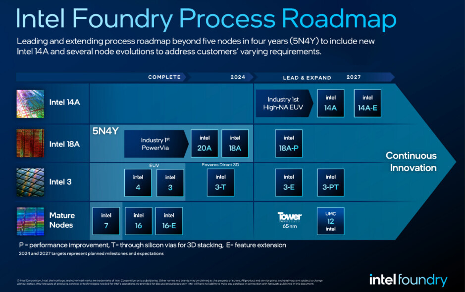
Intel is undergoing a transformation in its foundry strategy, aiming to compete strongly against rivals like TSMC and Samsung. Led by Pat Gelsinger, Intel recently reorganized its units into Intel Product and Intel Foundry. At the SPIE 2024 conference for optics and photonics, Anne Kelleher, Intel's senior vice president, announced that the 14A (1.4 nm) process offers a 15% improvement in performance-per-watt compared to the company's 18A (1.8 nanometers) process. The enhanced 14A-E process also provides an additional 5% performance boost over the regular A14 node. Intel's 14A process will be the first to utilize High-NA extreme ultraviolet (EUV) equipment, resulting in a 20% increase in transistor logic density compared to the 18A node.
Intel's aggressive pursuit of next-generation processes poses a significant challenge to Samsung Electronics, currently holding the second position in the foundry market. Through its IDM 2.0 strategy, Intel aims to regain its leading position in the foundry market and surpass Samsung by 2030. Collaborations with American companies like Microsoft further support Intel's ambitions. Intel has already secured a $15 billion chip production contract with Microsoft for its 1.8 nm 18A process. The semiconductor industry is closely watching Intel's progress, as advancements in process technology could reshape the competitive landscape. With Samsung planning to mass-produce 2 nm process products next year, the competition for dominance in the foundry market is intensifying.